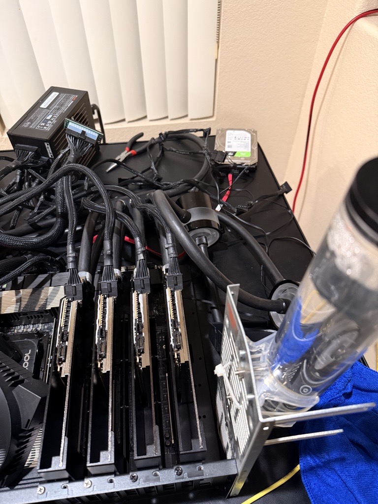
I built this rig to train models. Four RTX PRO 6000 Blackwells at 600 W each, 2.4 kW of heat in one chassis. Air coolers handle that fine for an inference burst, but a training run lasts two or three days, and air can’t keep up over that distance. The fans get unbearable. Exhaust from one card warms the next. And in synchronous training, the slowest card sets the pace, so whichever one throttles first drags the whole run down.
So I waterblocked the cards. I did one card first as a pilot, ran it for a week under real workloads, then planned to do the other three. The pilot is the reason this post exists. It failed at the end of that week, and the way it failed changed how I did the next three.
The rig
- 4× RTX PRO 6000 Blackwell Workstation (GB202, 96 GB GDDR7, 600 W)
- Threadripper Pro 7995WX on WRX90
- 4× Bykski full-cover waterblocks
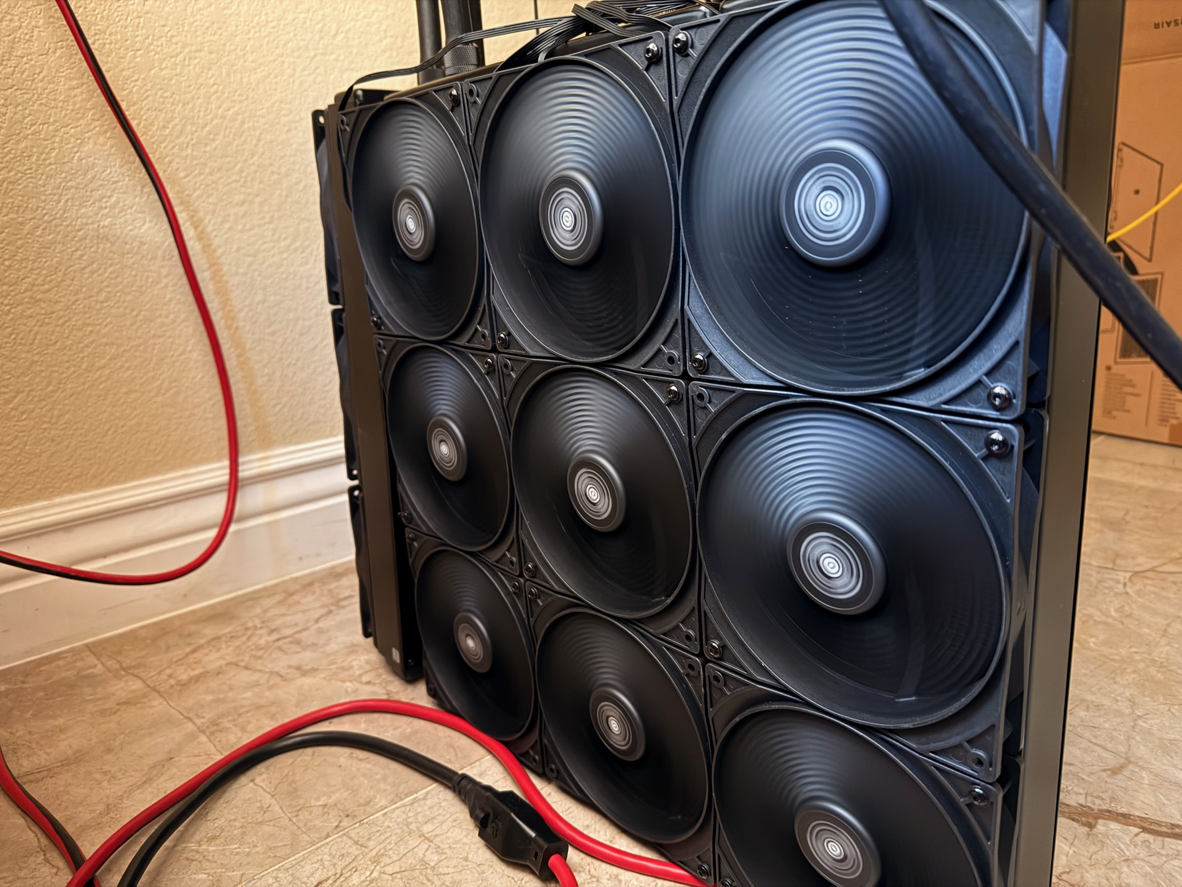
- Custom loop: one distro/reservoir, two pumps, distilled water, two Alphacool NexXxoS XT45 Full Copper 1260 mm Super Nova radiators (9× 140 mm fans each), GPUs plumbed in parallel
- 2× 1500 W PSUs (3 kW budget) for the ~2.4 kW sustained draw. The wall circuit also got upgraded mid-build after an early all-cards-down event under load.
That’s one radiator. There are two.
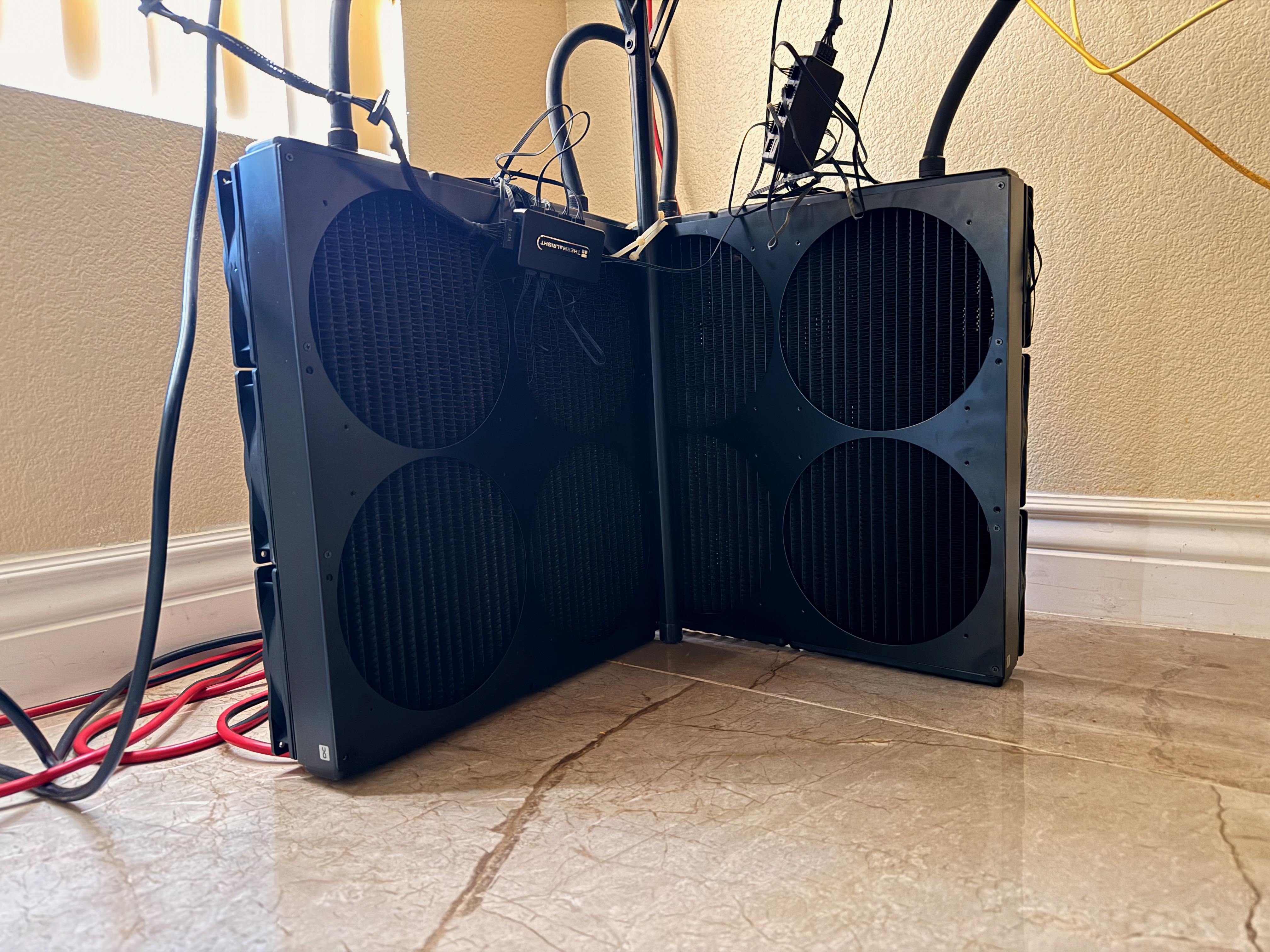
You don’t need this much radiator to dump 2.4 kW. I went overkill on purpose. Training runs are 24 to 72 hours of continuous load, and the loop doesn’t get a break between bursts the way an inference workload would let it. Big rads mean low-RPM fans, which means I can sleep next to the rig. Extra surface area is also insurance against a fan failing or a dust filter clogging in the middle of a long job.
The waterblock installs themselves are routine. Pull the stock cooler, clean the die, paste, pads on memory and VRMs, torque the block in a star pattern. The catch on these cards is the backplate. The GDDR7 packages on the back also need cooling. You either run pads against the case panel or bond small finned heatsinks on with thermal adhesive.
The pilot card
The first card went into the loop alone. The other three were still on air. The idea was to convert one, soak-test for a week, and only commit to the rest if it held up.
For about a week, it held up. Training and inference, full load, no Xids. Then it started falling off the bus. It was fine at idle and on short bursts. Anything sustained, and it would drop out partway through. The dmesg signature was the same every time:
NVRM: Xid (PCI:0000:02:00): 79, pid='<unknown>', GPU has fallen off the bus.
NVRM: Xid (PCI:0000:02:00): 154, Node Reboot Required
Xid 79 on its own is generic. It can be driver, PCIe link, power, or the card. The companion 154 and the PCIe AER logs were the actual signal: a DPC containment event. The root port killed the link because the card stopped acknowledging transactions. That points at the card or the power going to it, not at anything software-side.
What made it hard was that the card looked healthy. It enumerated, loaded the driver, ran short benchmarks. The failure only showed up after the VRMs had been pushing real current for a while.
The temptation here is to keep poking software. Try a different driver, swap CUDA versions, blame torch.compile. I did some of that. None of it changed anything. The signature was telling me to stop guessing and open the card up.
Pulling the block
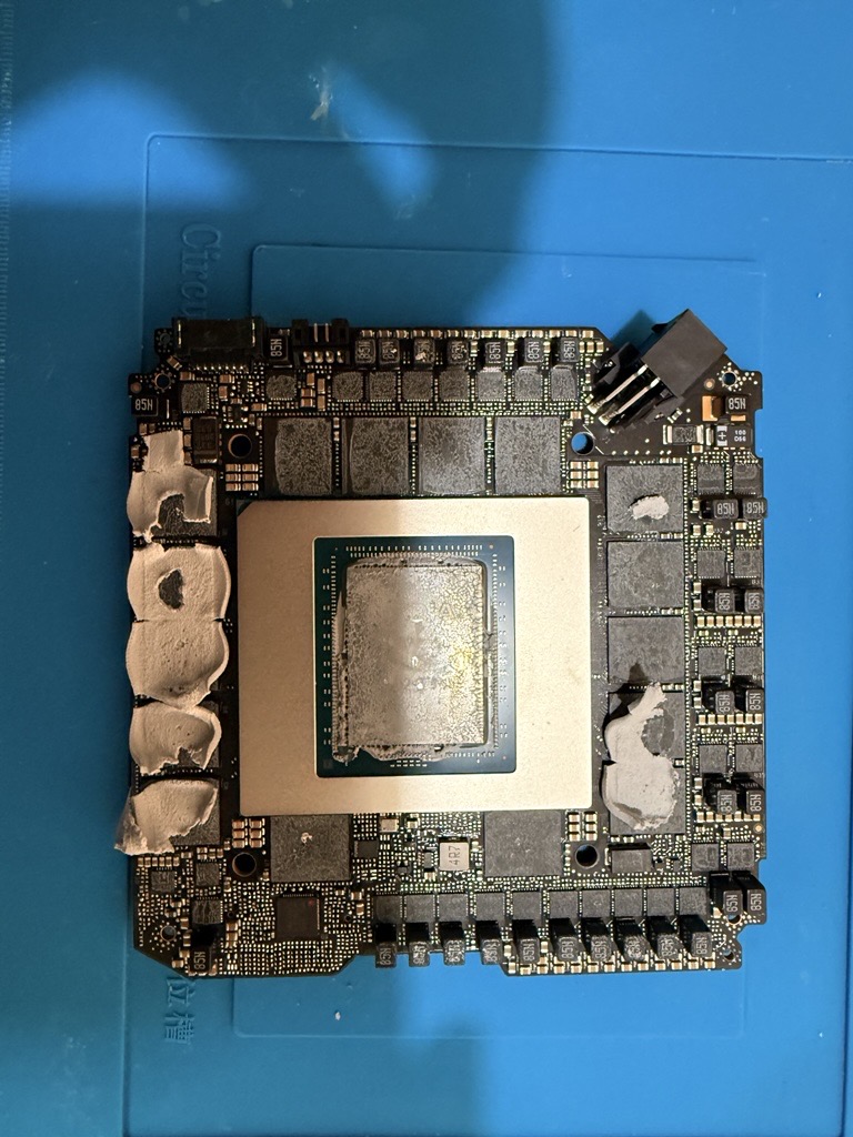
That’s the back of the GPU with the block off. The big metal lid in the middle is the GB202 IHS. The black ring around it is the VRM. Each of those little black squares marked 85N is a power inductor, a choke. They sit between the VRM MOSFETs and the GPU core, smoothing the switched current that feeds the die. A 600 W card has a lot of them so they can share the load. Lose one and the others pick up the slack, but the regulator’s feedback loop gets noisier and the rails get less stable.
Here is the part I would do differently if I were doing it again. I pulled the block at room temperature. The card had been sitting powered-off for a few hours, the loop was drained, everything was cool to the touch. I peeled the thermal pads off the VRM area. The pads came up. So did one of the chokes.
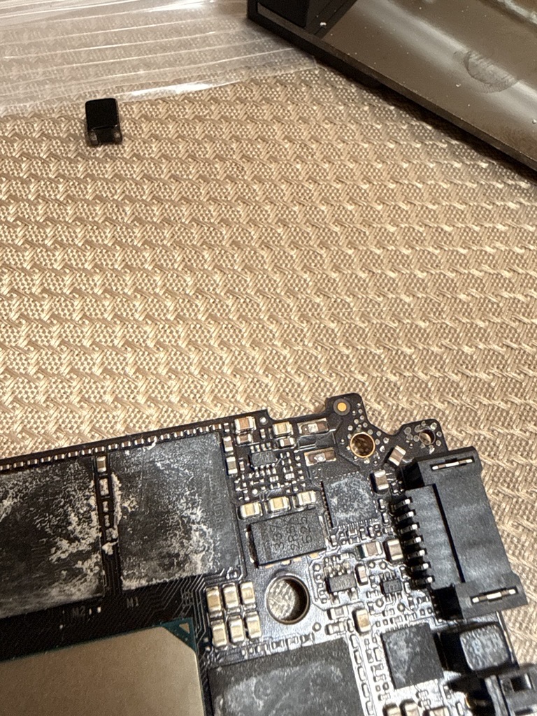
In the upper-right cluster, one footprint is empty. Two bare solder lands. The part that should bridge them is gone.
The part
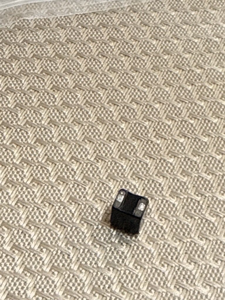
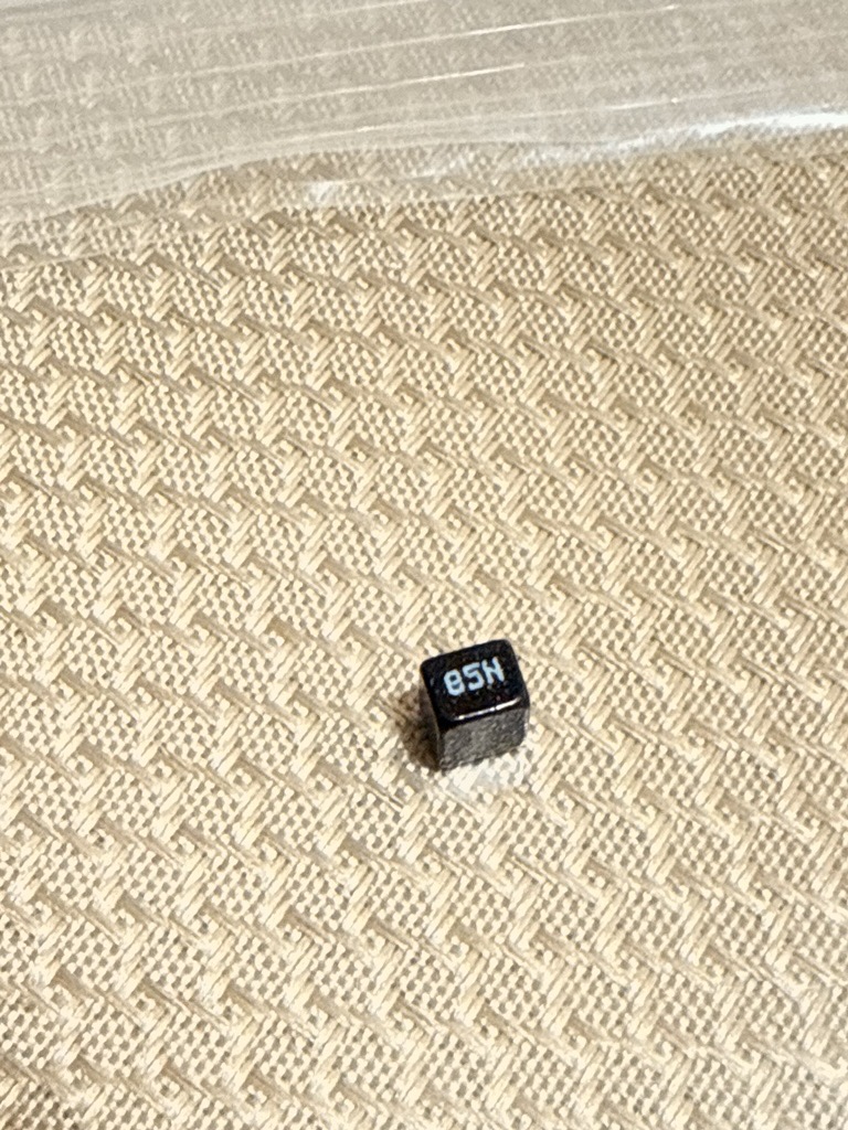
It’s about 3 mm on a side, marked 85N, identical to the 23 still on the board. A healthy SMD joint does not let go because of pad adhesion. You have to push pretty hard with a tool to lift one of these. So the fact that this one came up with the pad means the solder under it was already cracked.
That cracked joint is the whole story. The card had passed bring-up and run fine at light loads for a week. Once it had spent enough hours pulling 600 W, thermal cycling on a marginal joint widened the crack until the inductor lost reliable contact under transient current. With one inductor effectively missing under load, the others carried its share. The regulator’s feedback loop got noisier, ripple climbed, one of the GPU’s internal rails dipped out of spec, and the card aborted the PCIe link rather than corrupt data. That’s the Xid 79 + DPC containment signature. It only shows up when the load is real and sustained.
Warm the card before you touch the pads
The cold teardown is what made the cracked joint visible. If the joint had been healthy, the same cold teardown could have been the thing that cracked it.
Thermal pads on these cards are sticky. The bond between a pad and the small SMD components underneath is real. When you peel a cold pad off a VRM area, the pad pulls upward on everything it’s stuck to, and the force concentrates on the small parts, not on the big inductor packages. A marginal joint gives way completely. A healthy joint gets stressed and might fail later.
The fix is to bring the card up to around 90 °C before you start. At that temperature the silicone in the pads goes pliable and lets go of the components instead of holding on and lifting. You don’t need a hot air gun or a heat plate. Run a brief compute load on the card, get it up to temp, power off, and immediately start the teardown. The card’s own heat is plenty.
I learned this the hard way on the pilot. The three cards I converted after it all came apart warm and went back together without surprises. No further incidents during conversion.
Putting it back
Resoldering a power inductor onto a multi-layer GPU PCB is real microsolder work. Small pads, fine-pitch neighbors, multi-layer copper that pulls heat out of the joint as fast as you can put it in. I did not try to do this myself.
I walked into a SmartFix shop in Las Vegas. SmartFix is a national chain of phone and electronics repair shops, and they list logic board repair on their website. I handed the bare PCB to their microsolder tech and watched him do it. $40, about twenty minutes. These places do BGA reballs and 0201-pitch work on iPhone boards every day. A 3 mm power inductor with two big flat pads is a five-minute job to them.
This is the part most people miss when they think a GPU is dead. If the failure is a single discrete component coming off the board, you do not need an RMA, a hot air rework station, or a $500 microscope. You need to find the nearest shop that lists “microsoldering” or “logic board repair.” Phone-repair chains, indie cell shops, console-repair places. They all have the skill. The bring-it-in-and-wait economics are different from ship-it-back-to-the-manufacturer in a way that matters.
Back home: fresh paste on the die, fresh pads on the VRMs, the block back down, into the loop. Then I converted the remaining three cards using the warm-up-before-disassembly procedure.
Powered on. nvidia-smi showed all four. Standard stress suite on the repaired card alone:
Inference (vLLM):   10,283 tok/s sustained over 26 rounds
Training (PyTorch): 5,389 tok/s, ~213 TFLOPS, peak 54 °C, 609 W
Xid events:         none
Then all four together, same suite, started at the same time:
                inference        training         peak temp    power
GPU 0           10,393 tok/s     210.5 TFLOPS     57 °C        612 W
GPU 1 (fixed)   10,234 tok/s     212.5 TFLOPS     54 °C        609 W
GPU 2           10,311 tok/s     208.3 TFLOPS     58 °C        608 W
GPU 3           10,143 tok/s     206.2 TFLOPS     58 °C        607 W
--------------------------------------------------------------------
Aggregate       41,081 tok/s     837.6 TFLOPS     58 °C       2.44 kW
Xid events: 0
The fixed card runs the coolest of the four because the paste and pads are the freshest. The other three are within 4% of each other on inference and within 3% on training, which is about as tight as fleet matching gets on stock silicon. On water, every card stays at full boost the whole time. On air, this same workload was throttling cards into the mid-80s °C and clocking them down.
Takeaways
- Warm the card before pulling thermal pads. If you only remember one thing from this post, remember this. Cold pads pull SMD parts off the PCB. Run a brief load to bring the card up to ~90 °C, power off, and start the teardown immediately. The three cards I did this way had zero issues.
- Convert one card first, then the rest. A week of real workloads on the pilot is what surfaced the cracked joint. If I had converted all four at once, I would have had four blocks to pull and four chances to make new defects in the process.
- A week of working is not proof of healthy hardware. A marginal SMD joint can pass bring-up and only fail after enough thermal cycles. “It worked yesterday” doesn’t carry weight.
- Xid 79 + DPC containment under sustained load on one card is a hardware signal. I burned a few hours on driver swaps, CUDA versions, and inference engine theories before I gave up and opened the card. I should have skipped that.
- Don’t RMA it, and don’t solder it yourself. A local phone-repair chain with a microsolder tech can put a 3 mm SMD part back on a GPU PCB in twenty minutes for the price of dinner. The skill is in your city. You just have to look.
What the rig is doing now
The headline workload is training. Multi-day BF16 runs, all four cards at 600 W, around 840 TFLOPS aggregate. Air cooling couldn’t hold that envelope. The cards throttle into the mid-80s, the slowest one gates the synchronous step, and effective TFLOPS sag over the course of a long run. On water, every card stays at full boost for the whole job and step times stay flat. That’s the entire point.
When the rig is idle between training jobs, it serves inference: a DP=4 vLLM deployment of Qwen3.6-27B, one instance per GPU, nginx load balancer in front, exposed through a Cloudflare tunnel. At 1,024 concurrent requests with 5,120-token outputs, it sustains around 8,000 output tokens per second, balanced to within 0.7% across the four endpoints, KV cache at 99.6%, every card at full 600 W. Same thermal envelope as a training step, different shape.
The 85N inductor is back where it belongs.